

Authors: Michael Adams (1) and Dr. David Bell (2)
Institution: (1) University of North Carolina at Chapel Hill, (2) Center for Nanoscale Systems, Department of Engineering and Applied Sciences, Harvard University
Date: May 2007
Abstract:
Conventional Electron-beam lithography is done using a Scanning Electron Microscope (SEM), with a resolution limit of ~10 nm[1]. However, there is continued need for higher resolution lithography. The goal of this project is to investigate higher resolution Electron-beam lithography using a Scanning Transmission Electron Microscope (STEM). In principle, the STEM has two main advantages: less scattering of incoming high energy electrons, and a smaller electron probe diameter. We have created 100nm wide trenches in PMMA resist, which are promising early results. Reducing the exposure of the resist will likely give higher resolution.
Introduction:
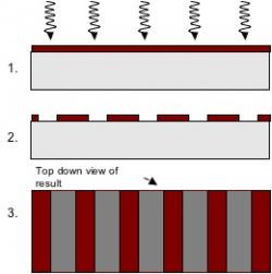
Lithography is the creation of three dimensional structures on a substrate that allows for transfer of a pattern to that substrate. First, a "resist",a material sensitive to light or electrons--is deposited on a substrate. Certain areas of the resist are "exposed" by light or electrons, making the area more susceptible to a subsequent chemical treatment, called "development". After development, the substrate has only certain places where it is still covered by resist. The substrate is etched or additional material is deposited (the remaining photoresist covers the area that is not meant to be etched or to have material deposited on it). Finally, the resist is stripped away, leaving the desired pattern in the substrate (see figure 1).
article_1025_order_0
There are two common lithography methods. The first, called Photolithography, is shining UV light through a plate with the proper pattern engraved in it, exposing light-sensitive resist beneath in the same pattern. This technique has a long history. In 1856, Joseph Niepce, of France, took the first photograph on a pewter plate, using oil of lavender and other ingredients. In 1935, Louis Minsk of Kodak developed the first synthetic photopolymer, one of the first negative resists. Finally, in 1940, Otto Suess developed the first diazoquinone-based positive photoresist.
In Photolithography, the limit of the smallest feature that can be produced (the resolution) depends linearly on the wavelength of light used. State of the art Deep UV photolithography using light wavelengths of 193nm has a resolution of ~50 nm[2]. However, for some applications, higher resolution is needed,for instance, for magnetic memory technology using an array of single domain magnetic pillars. Extremely small periodic structures are necessary for maximum storage density, with a pitch distance down to 30nm[1]. Thus, for these high resolution applications, another common lithography method is Electron-beam lithography.
Electron-beam lithography uses electrons instead of photons to expose a resist. Because electrons have a much smaller wavelength than the light used in photolithography, then Electron-beam lithography has a much higher intrinsic resolution. There is also a difference in that the electron beam can be focused onto substrate directly and controlled so it only exposes those areas which ought to be exposed, without needing a mask that blocks certain light from reaching certain areas. Conventional Electron-beam lithography is done using an SEM. The SEM can give electrons energies up to about 30 KeV, and use an electron probe with a diameter of a few nanometers. Due to scattering, however, the maximum resolution is about ~10nm[1].

article_1025_order_1
There are two main types of scattering,forward and back scattering. In forward scattering, the paths of the incoming electrons are deflected by the atoms' coulomb potential into a cone-like trajectory. In backscattering, the path is deflected by an angle greater than 90 degrees, and the electrons go back to expose a much larger area of the resist than the area of the incoming electron beam (see figure 2). The lower the electron energy, the more likely backscattering is to occur. The SEM has relatively low beam energy; thus, backscattering is an important problem. If two lines are written too close together, then the backscatter will end up exposing all the area in between. The TEM electron beam has a much higher energy, substantially reducing the backscatter. We can see this from the formula in Equation 1 for the Rutherford scattering cross section (with corrections for the relativistic speed of the electrons and the screening of effect of the electron cloud)
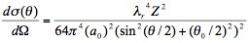
article_1025_order_5
where is the relativistically-corrected wavelength, is the bohr radius of the scattering atom, Z is the atomic number, and is the screening parameter, shown in Equation 2.

article_1025_order_6
. When the scattering angle is much greater than the screening parameter, we can neglect the electron-electron interactions, and we could drop the screening factor. More importantly, note that the wavelength, , is to the 4th power,higher energies imply smaller wavelengths, so as the TEM's electron beam has higher energies, the scattering cross section is dramatically reduced, so there is less backscatter. Therefore, lithography with the TEM or its cousin, the Scanning TEM (STEM), should have an inherently higher resolution than lithography using the SEM.
In the late 1980s, the STEM was tried for electron-beam lithography[3]. Early experiments with the STEM succeeded in producing patterns with resolution of ~10 nm[3]. Few groups have worked on this since, despite the availability of new Electron-beam resists. It was our purpose to further explore this idea by using a new resist, a high accelerating voltage in a STEM, and a thin sample. Furthermore, we wished to study ablation of a thin layer on the substrate by the electron beam, in a "direct writing" method.
A high energy electron beam can ablate metal, because the electron "collides" inelastically with the atoms of the sample, and loses some energy and momentum. We can express the energy transferred to the atom as Equation 3,

article_1025_order_7
where E is in eV, and is the angle through which the electron is deflected. Edgerton, et al [4] gives the expression for Emax as Equation 4,

article_1025_order_8
where E0 is also in eV, and A is the atomic mass number. If Emax >Es (the energy it takes to remove an atom from the surface), then the atom will leave the surface,the ablation takes place. As equation 4 shows, the higher the energy of the electron beam or lighter the atomic element, then the easier it is for an atom to be displaced from the surface.
Experimental Procedure:
We explored two different methods for writing with an STEM. The first was a lithography setup, where we spun coat an HMDS adhesion layer and then a layer of PMMA 495 C3 positive electron-beam resist on a 100nm thick silicon-nitride (Si3N4) membrane, and then used a JEOL 2010 STEM with a Nabity Pattern generator attached to expose the resist. We developed with MIBK 1:3 to clear away the exposed areas, and examined the patterns under the SEM. The idea behind using a silicon-nitride membrane is that this should reduce backscatter even more, thus potentially giving even cleaner, smaller lines.
The next method we tried was direct writing on a thin metal layer that was deposited on the 100nm Si3N4 membrane. The 200keV beam energy of our STEM should be enough to ablate the metal. We demonstrated this in principle by ablating holes in a Si3N4 membrane without a metal layer. We then thermally evaporated 10Å of Aluminum onto the Si3N4 membrane.
Results:
With our lithography setup, we have created some trenches in the PMMA resist (see figure 3). We would like to achieve finer resolution than demonstrated (about 100nm is the smallest line width), but this is an important first step.

article_1025_order_2
article_1025_order_3
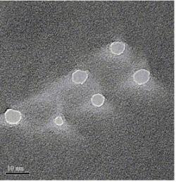
We ablated holes in a 100nm Si3N4 membrane (see figure 4). These were measured to be 3-7nm in diameter. This is a demonstration in principle of the STEM's ability to ablate metal and our ability to control the exposure of the sample to the electron beam in order to produce high resolution patterns.

article_1025_order_4
When we thermally evaporated 10Å of Aluminum onto the Si3N4 membrane, the metal did not adhere well enough to form a uniform layer; instead, the aluminum aggregated into clumps on the membrane surface. For better adhesion and a more uniform layer, we tried thermally evaporating 20nm of Chromium onto the membrane surface. This still clumped (see figure 5), making pattern writing impossible.
Discussion and Conclusions:
We successfully performed nanoscale electron beam lithography, creating 100nm wide trenches in PMMA polymer resist on a silicon-nitride membrane. However, it is evident not all trenches of the pattern that we attempted to create in the resist turned out correctly. Some of the trenches are sharply defined, but the center of the pattern is taken up by a huge hole in the resist where several trenches blended together. This suggests that one area for further study is the electron beam current dose used in the writing. We used doses between 1 and 16.5 nC/cm. However, given that our some of our lines have blended together, much lower doses may need to be explored. Another possibility is that the development step in the lithography process (where MIBK developer etches away areas of exposed resist on the membrane) is flawed. If the developer was left to etch the resist for too long, this may explain why too much of the resist is missing in some areas of the pattern. Thus, a shorter development time may also be necessary. A combination of these approaches may allow for creation of pattern where all trenches are sharply defined, without any overlap.
For demonstration purposes, we focused the 200keV electron beam on the 100nm thick Si3N4 membrane, and ablated holes through that. This is an important exhibition of the principle we hope to use in direct writing on metal deposited on the Si3N4 membrane--we expect that the STEM should be able to ablate the sufficiently thin layer of metal just as easily as it ablated holes through 100nm of Si3N4.
Unfortunately, attempts to create a uniform layer of metal on the Si3N4 membrane failed. As is clear from the results, thermal evaporation of thin layers of both aluminum and chromium did not produce uniform layers; instead, the metal aggregated into clumps on the surface of the membrane. We need to reduce the aggregation problem, and achieve a uniform layer in order to try the ablation step. There are several possibilities to investigate. Different metals could potentially be thermally deposited in a much more uniform way, or a different process altogether may be more appropriate,for instance, sputter coating the metal on the Si3N4 membrane may give the metal atoms enough energy to stick in place on the membrane, rather than allowing some to aggregate.
Acknowledgements:
Thanks to Dr. David Bell, Yuan Lu, Dr. Jiangdong Deng, Stephen Shepard of CNS. Thanks also to Kathryn Hollar of the Harvard REU program, and Melanie-Claire Mallison of the NNIN REU program.
References
[1] C. Vieu, F. Carcenac, A. Pepin, Y. Chen, et al, "Electron Beam Lithography: Resolution limits and applications", Applied Surface Science 164, 111-117, 2000 [2] Richard J. Blaikie, David O.S. Melville and Maan M. Alkaisi, "Super-resolution near-field lithography using planar silver lenses", Microelectronic Engineering 83 (4-9): 723-729 Apr-Sep 2006 [3] A.N. Broers, A.E. Timbs, R. Koch, "Nanolithography at 350 KV in a TEM", Microelectronic Engineering 9, 187-190, 1989 [4] Edgerton, R. F., Li, P., Malac, M., "Radiation Damage in the TEM and SEM", Micron 35, 399-409, 2004