

Author: Juliet Lawrence (1), Dr. Gary L. Harris (2), and James Griffin (3)
Institution: (1) Health and Humanity, University of Southern California, Howard Nanoscale Science and Engineering Facility (HNF), (2) Electrical Engineering, Howard University, (3) Electrical Engineering, Howard University
Date: May 2007
Abstract
Diseases such as retinitis pigmentosa and age-related macular degeneration lead to gradual loss of eyesight due to the progressive loss of retinal photoreceptors. Currently, several treatments for these diseases are being used to slow vision loss. One in particular hopes to restore partial vision by implanting an artificial retina using solar cells to provide electrical stimulation of the ganglion cells of the eye when exposed to light.
The objective of this work was to fabricate an AlGaAs/GaAs prosthetic retina with an array of 10μm diameter solar cells on a 3x3mm2 chip. Open circuit voltages of 0.82V were obtained under illumination for these cells. Mesas were etched into both sides of this chip to minimize electrical crosstalk between cells and minimize movement of the chip once implanted.
Introduction
Once light enters the eye it stimulates the retina's rods and cones. These are photoreceptors which are responsible for detail, low light and color vision. This light is then converted into electrical signals which are sent to the brain, via the optic nerve, and interpreted as vision[1]. There are several retinal diseases such as retinitis pigmentosa (RP) and age related macular degeneration (AMD) which disrupt the normal functions of the eye, more specifically the retina. RP is a genetic disorder which causes abnormalities of the retina's photoreceptors. AMD is a disease which causes loss of the sharp central vision needed to read or drive.
Since RP and AMP affect millions of people worldwide, strides are being made to slow down or stop their progression. Many researchers and practitioners believe that administering beta carotene (vitamin A), vitamins C, E and other nutrients can lower the risk of developing or slow down the progression of particular retinal diseases [2]. Also, patients are being treated with laser surgery and photodynamic therapy [2,3]. Lastly, many labs are developing artificial retinal implants (prosthetic retinas) to restore vision to patients. One very promising type of implant utilizes solar cell technology to provide electrical stimulation to the retina.
Many researchers, like those at Optobionics, are using silicon (Si) to make solar cell implants [4]. Though silicon-based implants have several advantages, such as being inexpensive, GaAs based solar cells are more efficient. By adding aluminum to GaAs, the spectral response can be tuned to resemble that of the human eye (Figure 1). A thin layer of AlGaAs near the surface serves as a window and helps decrease surface recombination, a process that causes charged carriers in the artificial retina to lose their ability to create the voltage and current needed to stimulate the eye.
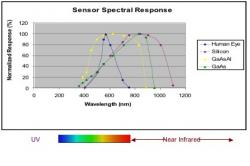
Figure 1: Sensor spectral response graph. The blue line, which peaks around 600 nm, represents the spectral response of the human eye while the purple line, peaking in the infrared region shows the spectral response of silicon. The yellow line represents the spectral response of GaAsAl which has a peak that encompasses that of the human eye.
Experiment
The fabrication of the prosthetic retina began with the growth of GaAs and AlGaAs layers by molecular beam epitaxy (MBE) on a 100µm thick n+ GaAs wafer. The first layer grown was an n+ GaAs buffer layer followed by a lower doped n+ GaAs layer. The third layer grown was p+ GaAs in order to create a p-n junction needed to power the cell. Next, a thin layer of p+ AlGaAs was grown and followed by a very thin cap layer of p+ GaAs (Figure 2). All n-type and p-type layers were doped with silicon and beryllium respectively.

Figure 2: Prosthetic retina structure. Each layer has a different doping concentration (see Table 1) to help the retina utilize as much sunlight as possible. This technique can result in much higher efficiencies.

Table 1: The left side of the table represents the contents of the five layers grown beginning with the substrate. The right side of the table contains the doping concentration of each layer grown. All n-type and p-type layers were doped with silicon and beryllium respectively.
After growth, metal contacts were evaporated onto both sides of a piece of the wafer and this piece was tested for cell efficiency (Figure 3). The bottom n-type contact was 20nm of germanium: 20nm of nickel: 200nm of gold. The top p-type contact was 40nm of titanium: 30nm of platinum: 100nm of gold. The contacts were then alloyed at 450ºC for 1 min. Fabrication of the prosthetic retina also involved making contacts to both sides. The bottom side contact was the same as mentioned above while the top contact was a 7nm thick layer of gold. The top contact was made semi-transparent to allow light to penetrate the cell.

Figure 3: Voltage vs Current graph of the prosthetic retina with no light (red line) and sunlight power of AM1 (blue line). The location where the blue line crosses x-axis is called the open circuit voltage and where the line crosses the y-axis is called the short circuit current.
The next step was to form mesas on the top surface by reactive ion etching (RIE). These mesas increase the prosthetic retina's efficiency in two ways. First, they decrease the amount of cross talk, stimulation of one cell by nearby cells, between the solar cells[5]. This will allow the artificial retina, which is composed of nearly two thousand solar cells, to have a higher resolution and yield a sharper image. The second purpose of the mesas is to allow the prosthetic retina to stay in place once implanted. This is made possible due to the phenomenon known as retinal cellular migration where retinal cells migrate into the empty spaces between the mesas which can be seen in Figure 4 [5,6].
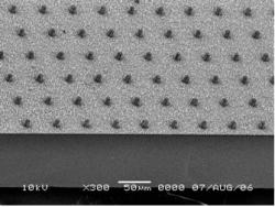
Figure 4: SEM image after 30 min of RIE w/photoresist mask. RIE etching produced vertical mesas (solar cells) that were approximately 10 µm high with vertical sidewalls and a very smooth surface.
The area that was not etched (an array 10µm diameter cells with a 50µm pitch) was masked with either a thick photoresist or metal layer. Two samples were prepared using photolithography. The first was masked with a 6µm thick layer of Microposit S1818 photoresist and the second was masked with 150nm of chrome and nickel. The sample masked with photoresist was exposed to 15 sccms of Cl2 at a pressure of 15 mtorr and 225watts of RF power for 30 minutes while the sample masked with metal was exposed to the same conditions for 45 minutes. After RIE, any remaining photoresist was removed by soaking or lightly brushing the sample with acetone. The metal mask was removed using a nickel and chrome etch. The chrome etch was made up of 5 parts HNO3 + 5 parts CH3COOH + 2 parts H2SO4 + 28 parts H2O (~ 0.25um/min at 25C) and was followed by a rinse in deionized water. The nickel etch consisted of 1 vol (1g NaOH, 2ml H2O) + 3 vol (1g K3[Fe(CN)6, 3ml H2O) also followed by a rinse in deionized water. Lastly, the sample was alloyed at 450°C to form ohmic contacts.
Results
After 45 minutes of etching the sample masked with metal had a mesa depth of approximately 18µm and vertical sidewalls as illustrated in Figure 5. The solution used to remove the metal mask caused further, unwanted, etching of the GaAs. The fill factor was calculated to be 0.52 and the solar cell efficiency was 5%. On the sample masked with S1818 photoresist, the 30 minute RIE produced a mesa depth of approximately 10µm with vertical sidewalls (Figure 5). Electrical measurements of the cell were taken under lighting conditions equivalent to AM1 to determine efficiency (ηs), fill factor (FF), short circuit current (Isc) and open circuit voltage (Voc).

Figure 5: SEM image after 45 min of RIE w/metal mask. RIE produced 18 µm deep sidewalls.
The maximum power: Pmax = IpVp (1)
The fill factor will be: FF= Pmax (2)
Isc Voc
The efficiency of the cell: ηs= Isc Voc FF (3)
Pm
Measurements showed the retina had a short circuit current of 2.1mA and an open circuit voltage of 0.82V. The final prosthetic retina was 2.5mm2 in size and consisted of roughly 1900 solar cells and is shown in Figure 6 next to a dime to provide a size comparison.
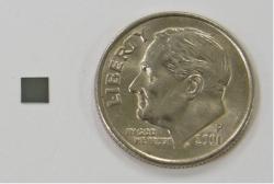
Figure 6: The final prosthetic retina device was 2.5 mm2 in size and consisted of roughly 1900 solar cells giving a resolution of 503 dots/inch. The device is next to a dime to provide a size comparison.
Discussion
Though RIE etching with a metal mask resulted in the vertical sidewalls and deep mesas, the additional GaAs etching that took place during mask removal would prevent the proper functioning of the prosthetic retina. The removal of the S1818 photoresist was much easier and didn't cause any further etching of our sample, this made it the best mask for the purposes of this experiment.
Previously, solar cells made from epilayer structures similar to the one used in this work yielded efficiencies as high as 20%. The 5% obtained in this work is well below what was expected. The reason for this low efficiency is not known and further testing will need to be done. However, electrical measurements taken on this cell structure yielded a high open circuit voltage. It should be noted that the efficiency of the final prosthetic device could not be measured because the 10µm cells were too small to contact.
In the future, RIE conditions need to be optimized to allow deeper and cleaner mesas. The AlGaAs/GaAs epilayer structure needs to be optimized to produce a higher efficiency. Redesign of the retina mask should also be done to more closely simulate the natural eye retinal geometry. Finally, an encapsulating layer will need to be developed before the device can implanted into the eye.
Acknowledgements
This research was sponsored by The National Science Foundation, the WIMS Center at University of Michigan, and the Howard Nanoscale Science and Engineering Facility.
References
[1] "eye, human." Encyclopædia Britannica. 2006. Encyclopædia Britannica Premium Service. 21 July 2006 [2] "Age related macular degeneration: what you should know", NEI Publication No. EY-01 [3] "Don't Lose Sight of Age-Related Macular Degeneration", NIH Publication No. 02-3462 [4] "The artificial silicon retina microchip for the treatment of vision loss from retinitis pigmentosa." Chow, Alan Y., et al. Archives of Opthalmology, vol. 122 No.4 460-469 (2004)
[5 ] " Attracting retinal cells to electrodes for high-resolution stimulation." Palanker, D., et al. Ophthalmic Technologies, SPIE vol.5314: 306-312 (2004).
[6] "Migration of retinal cells through a perforated membran; implications for a high- resolution prosthesis." Palanker, D., et al. Invest.Ophth.Vis.Sci., in press, 2004
[7] "GaAlAs/GaAs Heterojunction Prosthetic Retina." Stephanie Cheng. 2003 NNUN Research Accomplishments.