

Authors: Myranda Martin (1), Dr. Khalid Eid (2) and Dr. Jeffrey Catchmark (2)
Institution: (1) Lock Haven University of Pennsylvania, (2) Nanofabrication Department, Materials Research Institute, Pennsylvania State University
Date: May 2007
Abstract
The overall goal of this project was to fabricate very sensitive microbridge Superconducting QUantum Interference Devices, SQUIDs, using electron beam lithography followed by metal deposition and lift-off. The smallest lateral dimensions in the SQUID devices are those of the Josephson junction, which is 20 nm x 20 nm. Two electron beam resists were stacked in a bi-layer in order to get both ultrahigh resolution and good lift-off. The superconducting material was a 10 nm film of either niobium or aluminum. Niobium and aluminum become superconducting at temperatures below 9.26 K and 1.2 K respectively. Aluminum was deposited through thermal evaporation and niobium using ultrahigh vacuum sputtering, since it has a very high melting temperature for thermal evaporation. The SQUID rings were then characterized with detailed imaging using Field Emission Scanning Electron Microscopy (FESEM).
Introduction
A SQUID is a device used to measure very weak signals magnetic, specifically magnetic flux, and relies on the Josephson Effect. This effect refers to the behavior of a system consisting of a thin resistive or insulating layer sandwiched between two superconductors making a Josephson junction. A SQUID is typically a ring of superconductor interrupted by one or more Josephson junctions. One popular form of SQUIDs is known as a microbridge SQUID, where the superconducting ring is interrupted by two constrictions that form the two Josephson junctions as shown in Figure 1 (Fagaly 2006). Depending on the width and length of the constriction, the microbridge SQUID can be extremely sensitive to magnetic flux changes.

article_1027_order_0
Even though there are many devices capable of measuring magnetic fields, the SQUID is the most sensitive of all (Fagaly 2006). Many SQUIDs are sensitive enough to detect the subtle changes in the electromagnetic field of the human body. This is one reason why SQUIDs have many promising applications in the field of biomedical imaging. Magnetic Resonance Imaging (MRI) scanners currently offer non-invasive, high resolution images of internal organs and other soft-tissue areas of the body. But current clinical MRI scanners are expensive, mainly because they require large superconductive magnets and operate in a magnetic field around 1 tesla. Through the use of SQUIDs in MRI scanners, researchers have been able to produce high resolution images in the microtesla fields. The future application of SQUIDs in MRI scanners may mean less expensive clinical MRI scanners that continue to produce high resolution images (McDermott et al. 2004). Another application for SQUIDs in biomedical imaging is in magnetoencephalography (MEG). MEG is the process of measuring magnetic fields that enable brain imaging. SQUIDs placed in a device that is similar to a helmet can be used to detect and measure neural activity of the brain (Wakai 2004).
Other non-medical applications for SQUIDs may include the use of SQUIDs in military surveillance as well as other surveillance systems. This is due to the fact that any man-made object will have an effect or impact on the magnetic field of the environment surrounding the object. Therefore, a SQUID containing surveillance device would have the ability to detect this change in magnet field (Sensors and Measuring Techniques 2000).
SQUIDs have also been used thoroughly in studying magnetic materials. Microbridge SQUIDs were used to study the magnetic moment of Cobalt nano-particles having a 3nm diameter (Thirion et al, 2002). In this study nano-bridge SQUIDs were fabricated that should be sensitive enough to detect a single spin (i.e. the magnetic moment carried by a single electron). For this purpose ultrahigh resolution electron beam lithography were used to create nano-bridge SQUID rings with Josephson junctions about 20 nm in width.
Experimental Procedure
The project began by cleaning two 3" bare silicon wafers (from Silicon Quest). The wafers were cleaned with de-ionized water, acetone and isopropyl alcohol to remove any undesired residues. The wafers were dried with nitrogen and then placed on a hot plate at 180°C for five minutes to insure complete dehydration. Then two high resolution electron beam resists were spun and baked on to the wafers in a bi-layer configuration as follows: The bottom layer of Poly(methylmethacrylate-co-methacrylate acid) (P(MMA/MAA)) was spun then baked on a hot plate at 180°C for 3 minutes. The wafers were left to cool down to room temperature. Then the second e-beam resist ZEP520A (from Zeon Chemicals) was spun and baked at 180°C for 3 minutes. The first wafer was then exposed to the electron beam (e-beam) using a Leica EBPG-5HR e-beam lithography tool. An identical feature was exposed multiple times, each time in a different location and at a different dose, creating a "dose array". After e-beam exposure, the wafer was developed in n-amyl acetate for 2 minutes, methyl-isobutyl ketone: isopropyl alcohol (8:1) for 30 seconds, and de-ionized water for 30 seconds. Aluminum was then deposited onto the wafer using thermal evaporation in a Kurt Lesker evaporator. Lift-off then took place by immersing the sample in Microposit 1165 Nanoremover for 45 minutes at an elevated temperature. The final step was imaging the SQUID rings with FESEM to determine the optimal dose for the 20 nm features.
The second wafer was then exposed to the optimal dose obtained from the dose array. Identical SQUID features were written on the two halves of the wafer. The wafer was then developed and cleaved into two halves. Niobium was sputtered on one half of the sample and aluminum was thermally evaporated on the other. For each sample, the thickness of the metal deposited was 10 nm. Gentle ultrasonic agitation was used to promote the lifting-off of the metal. The two samples were then imaged with FESEM.
Results
From the dose array, an exposure of 180 µC/cm2 was found to be sufficient for the formation of the 20 nm lines in the Josephson junctions of the SQUID rings. Figure 2 shows three images from the dose array sample. The metal here is aluminum. Figure 2a shows an underexposed sample. In this figure the 20 nm channels are not continuous (i.e. the ring is incomplete) so the ring is not electrically connected. Figure 2b on the other hand, shows an over-exposed sample where the channel is wider than design. This will reduce the sensitivity of the SQUID device significantly. Figure 2c shows a sample with the optimal dose. The features are the right size and the lift-off is clean without any aluminum residue.

article_1027_order_1
article_1027_order_2

article_1027_order_3

article_1027_order_4
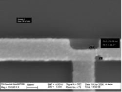
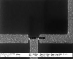
When making the actual samples (on the second wafer), aluminum samples worked very well giving a full and clean lift-off. Figure 3a shows an aluminum SQUID device with the two Josephson junction areas of about 20nm width. Figure 3b, on the other hand, shows a niobium SQUID after lift-off. The image shows that the inside area of the ring did not lift-off properly, even though the width of the junction area is approximately 20 nm.
article_1027_order_5
Discussion and Conclusions
Both niobium and aluminum films show grains of size as large as 50 nm, yet this grainy structure does not seem to have any significant impact on the lithography process. Even though the niobium and aluminum films were deposited on identical halves of the substrate, the niobium SQUID sample did not lift-off as well as the aluminum. This is due to the fact that niobium was sputtered while aluminum was thermally evaporated. Sputtering is known to be less collimated than thermal evaporation (Hasselbach et al. 2000) because it is done in argon gas with a background pressure larger than 1 mTorr. This inert gas atmosphere is necessary to knock out niobium atoms from the source target and have them deposited on the target substrate. But inert gas atoms will scatter the niobium atoms during their flight to the target, causing them to become uncollimated. Thermal deposition is done in high vacuum without any gases in the background and is more collimated than sputtering. A very light ultrasonic agitation helped promote the lift-off slightly in both types of samples.
In this study aluminum-based nanobridge SQUIDs were successfully fabricated with Josephson junction widths as small as 20 nm using electron beam lithography and a novel bilayer resist structure. The fabrication of niobium-based devices did not work as well as the aluminum based. This was because niobium was sputtered and aluminum was thermally evaporated; atoms impinging on the substrate are less collimated in sputtered films than in evaporated ones. Nano-bridge SQUIDs are very sensitive magnetic sensors and can potentially be used to detect single spins. More work needs to be done, to make the process compatible with sputtering as well as thermal evaporation. Testing of the devices will reveal their sensitivity limit.
Acknowledgements
I would like to thank the National Nanotechnology Infrastructure Network and the National Science Foundation for their funding and Penn State University for the use of their nanofabrication facility. I would like to thank my Principle Investigators Dr. Khalid Eid and Dr. Jeffrey Catchmark for their guidance and support. I would also like to thank Dr. Irfan Siddiqi for designing and optimizing the SQUID structures for maximum sensitivity. Finally, I would like to thank John McIntosh, Guy Lavallee, and Michael Rogosky without whom this would not have been possible.
References
Fagaly, RL. (2006) Rev. Scientific Instr. 77, 101101
Hasselbach, K et al. (2000) Superconductivity. Physica C 332: 140-147
McDermott, R et al. (2004) Microtesla MRI with a superconducting quantum interference device. Proceedings in the National Academy of Sciences of the United States of America 101: 7857-7861
Sensors and Measuring Techniques. 2000. Transferable European Space Technologies. 23 Dec. 2006 .
Thirion C. et al (2002) J. Magn. Magn. Mater. 242-245, 993-995
Wakai, R. (2004) Current and Future Technologies for Biomegnetism. AIP Conference Proceedings. 724: 14-19