

Author: David Toyli
Institution: University of Minnesota
Date: May 2007
Abstract
We have fabricated freestanding MnAs/GaAs nanowires using e-beam lithography and dry etching techniques. Nanowires as small as 75 nm in diameter were fabricated, with Magnetic Force Microscopy images of the nanowires showing the MnAs nanowire caps to be single-domain ferromagnets. The structures fabricated in this work hold promise for use in future studies of electrical spin transport.
Introduction
MnAs is an attractive material for use in studies of ferromagnet/semiconductor heterostructures. Its room-temperature ferromagnetic properties and its ease of growth by Molecular Beam Epitaxy (MBE) on arsenide semiconductors have motivated its use as a source of spin-polarized electrons in experiments in the field of spintronics (Wolf et al. 2001; Zutic et al. 2004). In this work we present results on the fabrication and characterization of MnAs/GaAs nanowires. Freestanding nanowires with diameters down to 75 nm were fabricated and Magnetic Force Microscopy (MFM) studies of nanowires with diameters down to 100 nm were conducted. Future experiments utilizing these nanostructures will provide information on the influence of geometrical confinement on the transport of spin-polarized electrons. Recent experiments on electron spin dynamics in InGaAs lateral channels have demonstrated one-dimensional electron spin dynamics in channels an order of magnitude greater than the electron mean free path (Holleitner et al. 2006). The structures fabricated in this work could be used to do electrical spin transport experiments in a vertical geometry to further understand the effects of reduced dimensionality on spin-polarized transport in semiconductors.
Method and Materials
The nanowires were processed from a thin film grown by MBE. The film consists of a 25 nm thick layer of Type-A MnAs (Tanaka 2002) on top of 1.5 μm of n-GaAs (n = 5.25 x 1017 cm-3) grown on a semi-insulating GaAs substrate. Superconducting QUantum Interference Device (SQUID) measurements showed the MnAs layer to have an easy-axis coercivity of approximately 200 Oe at 300 K. SQUID measurements done at 5 K show asymmetric hysteresis loops similar to those observed in exchange-biased systems (Chun et al. 2001; Ney et al. 2004).
The thin film samples were processed into freestanding nanowires using a two-step process. In the first step a pattern is defined on the sample surface via e-beam lithography. Using the negative maN-2403 e-beam resist as an etch mask, the pattern was transferred to the thin film via Reactive Ion Etch (RIE), creating arrays of nanowires with diameters from 75 nm to 500 nm. The RIE was conducted using a Cl2 and Ar gas mixture with gas flow rates of 1 and 20 sccm, respectively, while the RF power was 50 W and the chamber pressure was 10 mT.
The magnetic properties of the MnAs nanowire caps were investigated with an Asylum MFP-3D Atomic Force Microscope (AFM) using a magnetic cantilever tip. The AFM was used to take MFM images to characterize the ferromagnetic ground states of the MnAs caps. MFM images in an applied magnetic field were also taken with an Asylum Research Variable Field Module (VFM).
Results
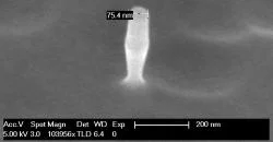
Freestanding nanowires with diameters down to 75 nm were successfully fabricated. Figure 1 shows a Scanning Electron Microscope (SEM) image of a 75nm diameter nanowire with a height of approximately 350 nm. The nanowire fabrication process was robust; typically 100% of the dots patterned during e-beam lithography were successfully etched into nanowires. Undercutting of the GaAs layer limited the nanowire heights,the greatest height to diameter aspect ratio achieved, determined by SEM imaging, was approximately 6 to 1 using a Cl2-based RIE recipe.
article_964_order_0
Magnetic characterization of the nanowire caps done by MFM showed ferromagnetic behavior in MnAs caps with diameters down to 100 nm (the 75 nm nanowires were not measured because this array was not located during imaging). Figure 2 shows three nanowires of diameter 500 nm and height 350 nm. The image shows the MnAs caps to be ferromagnetic. MFM scans also showed MnAs caps of diameter 500 nm to be either single-domain or multi-domain and showed MnAs caps of diameters less than 500 nm to be only single-domain. Previous studies of thicker MnAs nanostructures have shown MnAs nanodisks of diameters greater than 100 nm to be multi-domain (Takagaki et al. 2006). This result does not contradict our measurements since thicker MnAs nanodisks have a lower out-of-plane demagnetization energy, facilitating the formation of domain walls in the MnAs nanodisks. Fig. 3 shows an MFM scan of four 100 nm diameter nanowires. The MFM scan was done at a height of 275 nm above the sample surface to avoid contact with the nanowires. The large scan height results in poor resolution of the domain structure of the 100 nm MnAs caps. In order to obtain a better image of the MnAs caps the nanowires were placed in a magnetic field along the MnAs easy axis large enough to reverse the magnetization of the MFM tip but not large enough to reverse the magnetization of the MnAs caps. Figure 3 shows that the fringe fields around the MnAs caps invert after the magnetization of the MFM tip is flipped. This response suggests that the MnAs caps are ferromagnetic with a coercive field larger than the applied field.

article_964_order_1
Discussion
The samples fabricated in this work hold promise for use in future studies of electronic spin transport, although it is not known whether the 75 nm nanowires will have sufficient electronic confinement to produce one dimensional electron spin dynamics. Recent experiments on GaAs nanowires investigated by Kelvin Probe Microscopy (KPM) have demonstrated conductance plateaus which indicate the presence of a ferromagnetic phase in 20 nm wide GaAs nanowires (Crook et al. 2006). While KPM is able to produce and probe nanowires smaller than those produced using top-down fabrication methods, it should be noted that in the GaAs nanowires in this work the electron charge transport could occur within only a small region of the 75 nm diameter nanowires due to depletion of the exposed n-GaAs. It is also possible that the outer region of the GaAs nanowires could have become ion-damaged during the RIE, limiting the electron transport to inner portions of the wire. Such issues are left to be investigated in future experiments.

article_964_order_2
Future work will focus on using the MnAs/GaAs nanowires for studies of one-dimensional spin transport. Initial spin transport measurements could be done electrically at room temperature using a Conductive Atomic Force Microscope (CAFM) and a VFM. The CAFM measurements could be followed by low-temperature electrical measurements to provide a more complete understanding of spin transport in these nanowires. Such low-temperature measurements would require nanowires processed so that the MnAs caps are contacted with a metal electrode. Processing these nanowires entails conformally coating the nanowires with a dielectric, planarizing between the nanowires using a spin-on dielectric like polyimide, and then etching to free the MnAs caps for metal evaporation. The purpose of the conformal dielectric coating is to structurally enhance the nanowires, as it was determined that the freestanding nanowires break at spin speeds greater than 3 krpm.
Acknowledgements
David Toyli would like to acknowledge Professor David Awschalom and Jesse Berezovsky for their guidance and support in completing this project and acknowledge Shawn Mack and Roberto Myers for sample growth. This work was supported by the NSF, the NNIN, and DARPA.
References
Chun, S.H. et al. (2001) Intrinsic exchange biasing in MnAs epilayers grown on (001) GaAs. Applied Physics Letters 78: 2530-2532.
Crook, R. et al. (2006) Conductance Quantization at a Half-Integer Plateau in a Symmetric GaAs Quantum Wire. Science 312: 1359-1362.
Holleitner, A.W. et al. (2006) Suppression of Spin Relaxation in Submicron InGaAs Wires. Physical Review Letters 97: 036805.
Ney, A. et al. (2004) Nature of the magnetic and structural phase transition in MnAs/GaAs(001). Physical Review B 69: 081306.
Takagaki, Y. et al. (2006) First-order phase transition in MnAs disks on GaAs (001). Physical Review B 73: 125324.
Tanaka, Masaaki (2002) Ferromagnet (MnAs)/III-V semiconductor hybrid structures. Semiconductor Science and Technology 17: 327-341.
Wolf, S.A. et al. (2001) Spintronics: A Spin-Based Vision for the Future. Science 294: 1488-1495.
Zutic, Igor et al. (2005) Spintronics: Fundamentals and Applications. Reviews of Modern Physics 76: 323-410.